SCG102A-DFC-A1P6 V1.0 数据手册
SCG102A
Synchronous Clock
Generators
PLL
2111 Comprehensive Drive
Aurora, Illinois 60505
Phone: 630- 851- 4722
Fax: 630- 851- 5040
www.conwin.com
Applications
• SONET / SDH / ATM
• DWDM / FDM
• DSL-PON Interconnects
• FEC (Forward Error Correction)
Features
• 3.3V High Precision PLL
• Accepts 1 of 4 Selectable, Pre-determined Input Frequencies
• 77.76 MHz to 170 MHz Output Frequencies Available.
• Jitter Generation OC-192 Compliant
• 1.0” x 0.80” x 0.285”, Surface Mount
Bulletin
Page
Revision
Date
Issued By
SG076
1 of 8
00
11 APR 07
ENG
�General Description
The SCG102A provides high precision phase lock loop
frequency translation for the telecommunication applications.
The SCG102A product generates LVPECL outputs from an
intrinsically low jitter, voltage controlled crystal oscillator.
SCG102A is well suited for use in line cards, service
termination cards and similar functions to provide reliable
reference, phase locked, synchronization for TDM, PDH, SONET
and SDH network equipment . The SCG102A provides a jitter
filtered, wander following output signal sychronized to a superior
Stratum or peer input reference signal.
The SCG102A includes a lock detect alarm output. The PLL
control voltage is brought out through a 470 kΩ restistor and can
be used to determine when the pull range limits are reached.The
LVPECL outputs may be put into the tri-state high impedance
condition for external testing purposes by asserting a high signal
to the Enable/Disable pin.
The SCG102A is a 3.3 Volt component that will typically draw
75mA. The SCG102A is designed to be used in applications that
require temperature rating of -40°C - 85° C. The SCG102A
package typical dimensions are 1.0” x 0.80” x 0.285” (See fig. 2
for maximum dimensions). Parts are assembled using high
temperature solder to withstand surface mount reflow process.
The SCG102A locks to any one of four pred-determined input
frequencies selected using the SELECT (A&B) lines (See Table
4). The output may be any single frequency from 77.76 MHz to
170 MHZ.
Functional Block Diagram
Figure 1
LD
470 kΩ
(Pin 3)
Monitor
(Pin 4)
CLKIN
Frequency
Loop
PECL
OUT
Divider
Filter
VCXO
COut
(Pin 1)
(Pin 9)
(Pin 10)
Frequency
10 kΩ
Divider
Select A
(Pin 12)
Microprocessor
Select B
(Pin 13)
Enable/Disable
10 kΩ
(Pin 8)
Absolute Maximum Rating
Table 1
Symbol
Parameter
Minimum
Vcc
Power Supply Voltage
VI
Input Voltage
Ts
Storage Temperature
Nominal
Maximum
Units
-0.3
5.5
Volts
-0.3
Vcc
Volts
-55
125
°C
Data Sheet #: SG076
Page 2 of 8
Notes
Rev: 00
Date: 4/11/07
© Copyright 2007 The Connor-Winfield Corp. All Rights Reserved Specifications subject to change without notice
�Specifications
Table 2
Symbol
Parameter
Minimum
fIN
Available Input Frequencies CMOS
PECL
fOUT
Vcc
Nominal
Maximum
Units
8k
1M
100 M
100 M
Hz
Hz
Output Frequencies(LVPECL)
77.76 M
170 M
Hz
Supply Voltage
3.135
3.3
3.465
Volts
100
mA
ICC
Supply Current
75
CLKIN
Input Logic
CMOS
PECL
CLKOUT
Output Logic F = Comp. PECL
A = CMOS
D = PECL
1
PECL
VOH
2.275
V
VOL
TR/TF
Rise/Fall Time
SYM
Output Symmetry
BW
Bandwidth
20
JGEN
Jitter Generation RMS
(12 kHz - 20 MHz)
0.5
JTRAN
Jitter Transfer
APR
Input Frequency Tracking
TOP
Operating Temperature
NOTES:
Notes
0.5
45
1.68
V
1
ns
55
%
Hz
1
ps
0.1
dB
±50
F=
C=
-40
0
2
ppm
85
70
°C
°C
1.0: Only HCMOS and LVHCMOS is supported for input frequencies < 1MHz
2.0: GR-253-CORE, Sec. 5.6.2.1.2
Pin Description
Table 3
Pin #
Connection
Description
1
CLKIN
Input Frequency - The SCG102A AC couples the input , this means that the unit is
capable of handling HCMOS, LVCMOS, PECL, LVPECL input signals.
2
GND
Ground
3
Lock Detector
Logic “1” indicates that the unit is locked to the input reference
Logic “0” indicates that the reference is lost or out of lock range
4
VCXO Monitor
Control voltage level for the PECL oscillator (Between 0.3V and 3.0V when locked)
5
----
Missing
6
NC
No connection
7
GND
Ground
8
Enable/Disable
Logic “0” (or no connect) = Output Enabled
Logic “1”
= Output Disabled (Tri-Stated)
9
Out
Output
10
COut
Complementary Output
11
NC
No connection
12
Select A
Input Frequency Select Control Pin. See Table 4.
13
Select B
Input Frequency Select Control Pin. See Table 4.
14
NC
No connection
15
GND
Ground
16
VCC
Power supply voltage (3.3 Vdc ± 5%)
Data Sheet #: SG076
Page 3 of 8
Rev: 00
Date: 4/11/07
© Copyright 2007 The Connor-Winfield Corp. All Rights Reserved Specifications subject to change without notice
�Input Frequency Selection
Table 4
Input Freq
SEL A
SEL B
f1
0
0
f2
0
1
f3
1
0
f4
1
1
Output Load and Power Supply Filtering Recommendations
Figure 2
*
*
* It is highly recommended
*
that either a linear regulator
or bypass capacitors be
used. Typical values would
be 10 uF, 0.1 uF, 100 pF.
VT -2 VDC
LD
(Pin 3)
470 kΩ
Monitor
(Pin 4)
CLKIN
Frequency
Loop
PECL
OUT
Divider
Filter
VCXO
COut
(Pin 1)
50Ω
50Ω
(Pin 9)
(FOUT)
(Pin 10)
Frequency
10 kΩ
Divider
Select A
(Pin 12)
Microprocessor
Select B
(Pin 13)
10 kΩ
Enable/Disable
(Pin 8)
Data Sheet #: SG076
Page 4 of 8
Rev: 00
Date: 4/11/07
© Copyright 2007 The Connor-Winfield Corp. All Rights Reserved Specifications subject to change without notice
�Ordering Information
Table 5
10 MHz
10 kHz
8 kHz
16 kHz
64 kHz
1.024 MHz
1.048 MHz
1.544 MHz
2.048 MHz
4.096 MHz
A
B
C
D
E
F
G
H
J
K
8.192 MHz
13.00 MHz
16.384 MHz
19.44 MHz
20.48 MHz
26.00 MHz
27.00 MHz
38.88 MHz
44.736 MHz
53.10468 MHz
L
M
N
P
R
T
W
X
Y
Z
51.84 MHz
61.44 MHz
77.76 MHz
82.944 MHz
112.00 MHz
139.264 MHz
155.52 MHz
166.6286 MHz
114.0 MHz
125.0 MHz
0
1
2
3
4
5
6
7
8
9
For any model, the reference inputs and output frequency must have a common frequency of 2.667Hz (8kHz/3)
Ex 1: A Model with reference inputs of 8kHz, 16kHz, 32kHz and 64kHz with a Output frequency of 155.52MHz is valid due to the
common frequency of 2.667kHz. Contact CW regarding models that do not have a input/output common frequency of 2.667kHz.
SCG102A- D F F - A 1 P 6
Output Frequency (2 to 9)
See chart above. If a custom frequency
is desired, enter S followed by the
frequency. Contact a sales
representative for the availabilty of
custom frequencies.
Input Frequency (A to 9)
See chart above.
If more than one frequency is desired,
enter S and list all desired frequencies.
Contact a sales representative for the
availabilty of custom frequencies.
Supply Voltage
D = 3.3 VDC ± 5%
Output Type
F = Comp. PECL
Temperature Range
C = 0°C to 70°C
F = -40°C to 85°C
Number of Input Frequencies
1 = 1 Input Frequency
2 = 2 Input Frequencies
3 = 3 Input Frequencies
4 = 4 Input Frequencies
Sample Part Number Examples:
SCG-102A- DFF-A1C2
SCG-102A- DFF-A4S2, S = 8 kHz, 16.384 MHz, 19.44 MHz, 38.88 MHz
SCG-102A-DFF-D1ZS, S = Custom Frequency
Data Sheet #: SG076
Input Logic
A = CMOS
D = PECL
Page 5 of 8
Rev: 00
Date: 4/11/07
© Copyright 2007 The Connor-Winfield Corp. All Rights Reserved Specifications subject to change without notice
�Package Dimensions
Recommended Footprint Dimensions
Figure 3
Figure 4
.100 [2.54mm]
1.000 [25.40mm]
PIN 1
.740 [18.80mm]
.285 [7.24mm]
MAX.
.800 [20.32mm]
Solder Profile
Figure 5
300
Peak Temp.
245°-255°C for 15 sec Typ.
250
221°C
Temp (°C)
200
Reflow Zone
30/90 sec
(Min/Max)
150
Soaking Zone
60-90 sec Typ.
(2 min Max)
100
50
Ramp Slope not
to exceed
±3°C/sec
0
0
50
100
150
200
250
300
350
Time (sec)
Data Sheet #: SG076
Page 6 of 8
Rev: 00
Date: 4/11/07
© Copyright 2007 The Connor-Winfield Corp. All Rights Reserved Specifications subject to change without notice
�Data Sheet #: SG076
Page 7 of 8
Rev: 00
Date: 4/11/07
© Copyright 2007 The Connor-Winfield Corp. All Rights Reserved Specifications subject to change without notice
�2111 Comprehensive Drive
Aurora, Illinois 60505
Phone: 630- 851- 4722
Fax: 630- 851- 5040
www.conwin.com
Revision
Revision Date
Note
00
4/11/07
Final Release
�
SCG102A-DFC-A1P6 V1.0 价格&库存
很抱歉,暂时无法提供与“SCG102A-DFC-A1P6 V1.0”相匹配的价格&库存,您可以联系我们找货
免费人工找货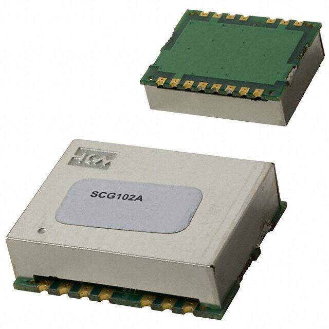


 工商网监
湘ICP备2023018690号
工商网监
湘ICP备2023018690号